Companies who trust us


About yieldWerx
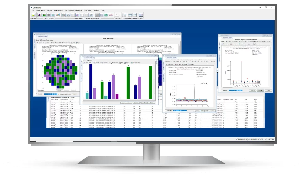
yieldWerx delivers end-to-end semiconductor analytics for improved decision-making and process enhancement, covering panel inspection to advanced packaging. As a data analytics service, it empowers IDMs, Equipment Manufacturers, Fabless Companies, and OSATs with actionable insights, benefiting startups to industry leaders.
- Automated Data Loading
- Raw Data Monitoring
- Reporting & Analysis
- Standard Data Access For External Tools
- Yield Calculation Flexibility
- Data Archive/Purge Module
- Assembly Map Generation
- Lot Genealogy
- Executive Dashboards, Data warehouse Reporting
- Wafer/Reticle Map Definition Tool
- Part Average Test (PAT)
- Smart Wafer Map Merge Module
- SPC/SBL/SYL
- Real Time PAT Final Test
- Inspection Image Management
- Memory/Optical Bit Map Analysis
- SMART Probe
- Defect Data Management
- Wafer Bank/Scrapping/Down Grading Management
- OEE Management
- Test Program Management (TPM)
We support WAT/PCM data from more than 15 foundries, including:
- TSMC
- Tower
- SMIC
- Global Foundries
- IBM
- UMC
- And many others
We support data from the several leading assembly and test houses, including:
- Stats Chip PAC
- UTAC
- Amkor
- ISE Labs
- ASAT
- Carsem
- DA-Integrated
- ASE
- KYEC
- And many others
We support data from all leading semiconductor test equipment manufacturers, including:
- Teradyne
- Eagle
- LTX/Credence
- Advantest
- Keithly
- And several others
yieldWerx’s customizable yield management experts can complement your product engineering teams with services that include:
- Data cleansing and loading into yieldWerx
- Data scientists applying proven methodologies and best practices for outlier detection, test escape, etc.
- Providing actionable insights and recommendations to Product, Quality, and Test Engineering teams
A Trusted Partner for thousands of
Empowering data-driven decision-making: yieldWerx's pioneering semiconductor yield analysis solution offers immediate
advantages to startups with big dreams and leading companies in the semiconductor industry.
Explore yieldWerx Yield Management Systems
OPERATIONS______
PRODUCT ENGINEERING
TEST ENGINEERING______
QUALITY AND RELIABILITY
Lets crack some numbers
We have helped achieve maximum yield by yield analysis software with minimal effort for millions of products.
Devices analyzed per year
users
satisfied clients
up to
cost savings

Industries Served
Aerospace & Defense

Automotive & Life Sciences
Consumer Products
Fabless Companies
OSAT
Blogs

A Guide to Implementing Yield Management Software in the Semiconductor Industry
Optimizing yield is essential for operational efficiency and financial success. Yield management software significantly addresses these challenges, utilizing data analytics and machine learning to improve defect detection and process control….

Best Practices for Sensing Failures in Automotive ICs
The integration of semiconductor integrated circuits (ICs) in automotive systems has significantly advanced vehicle functionality and performance. These ICs are vital for a broad range of operations, from engine management…

Why is Semiconductor Wafer Inspection Important?
Wafer inspection is one of the most remarkable steps in the production of semiconductor devices, as it verifies the accuracy and functionality of the wafers, which serve as the basis…
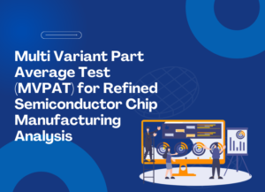
Multi Variant Part Average Test (MVPAT) for Refined Semiconductor Chip Manufacturing Analysis
The Multi Variant Part Average Test (MVPAT) is an innovative chip manufacturing analysis approach focusing on advanced quality control through multivariate testing and data-driven manufacturing, particularly for automotive electronics. MVPAT…
Frequently Asked Questions
Semiconductor yield management software has essential capabilities for semiconductor manufacturers to track, assess, and enhance their production efficiency and profitability. Users can utilize various modules, including Automated Data Loading, Reporting & Analysis, Data Archive, and more.
Yield analysis plays a fundamental role in semiconductor fabrication, enabling manufacturers to pinpoint, scrutinize, and rectify variations or disruptions in production, thereby ensuring consistent quality and profitability.
Absolutely, predictive analytics can significantly optimize yields for manufacturers by utilizing past and current data to predict future trends, evade potential disruptions, and refine manufacturing processes.
Yield management software conserves engineering time by automating various tasks and providing insightful data, minimizing the time engineers dedicate to manual operations and data interpretation.
The Yield Manager serves as a fundamental component of factory control, managing the entire yield management process, including in-line process control, defect inspection, and the logistics of materials and analysis.
The software guarantees quality by offering extensive tools for categorizing defects, conducting inspections, and providing metrology solutions. It also ensures that each device adheres to industry benchmarks before distribution.
yieldWerx allows clients to view and test limits if necessary, ensuring that regulatory requirements are met. The platform helps in identifying problematic parts of integrated circuits (ICs) and improving overall yield. By analyzing data and identifying the most problematic areas, clients can take targeted actions to improve yield and ensure compliance with regulatory standards.
yieldWerx enables clients to monitor and analyze all aspects of test results, ensuring consistent quality in microcontroller manufacturing. The platform automatically loads processed data into relevant databases and tags them by data source, providing a simple overview of test activities and enabling end-to-end data traceability. Ready-made graphs and analysis tools help identify long-term trends and flag wafers with significant deviations from normal behavior.
Manufacturers can employ the software for immediate monitoring, yield analysis, predictive maintenance, and process optimization, leading to substantial yield amplification and cost efficiency in manufacturing operations.